
Views: 4 Author: Site Editor Publish Time: 2020-08-29 Origin: Site


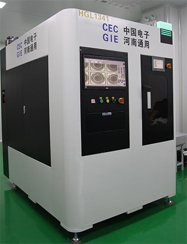
Good news from our country's scientific research field! China Great Wall Technology Group officially announced that its subsidiary Zhengzhou Rail Transit Information Technology Research Institute and Henan General Intelligent Equipment Co., Ltd. have jointly tackled key problems for one year. my country’s first semiconductor laser invisible wafer cutting machine has been successfully developed on May 8. Domestically, it has achieved the best light wave and cutting technology, and is at the international leading level in key performance parameters.
Great Wall of China stated that this marks a substantial breakthrough in my country's semiconductor laser invisible wafer cutting technology, and the dependence on imports of related equipment is about to break, opening the prelude to the development of my country's laser wafer cutting industry.
It is reported that Zhengzhou Rail Transit Institute was established in 2017. For several years, it has been carrying out scientific research and innovation and technological breakthroughs around independent safety industrial controllers, high-end equipment manufacturing, and new generation information technology breakthroughs. After being acquired by a company under China Great Wall, it has entered a new one. Accelerate the development period.
According to reports, wafer cutting is an indispensable key process in the semiconductor packaging and testing process. Compared with traditional cutting methods, laser cutting is a non-contact processing, which can avoid damage to the crystalline silicon surface and has high processing accuracy. , High processing efficiency, etc., which can greatly improve the quality, efficiency and benefit of chip manufacturing.
The first semiconductor laser invisible wafer cutting machine in my country adopts special materials, special structure design and special motion platform, which can realize the high stability and high precision of the processing platform during high-speed motion. The motion speed can reach 500mm/s and the efficiency Much higher than foreign equipment.

In terms of optics, according to the spectral characteristics of monocrystalline silicon and the application level of industrial lasers, this equipment uses lasers with appropriate wavelength, total power, pulse width and repetition frequency to finally achieve invisible cutting.
In terms of images, cameras with different pixel sizes and different photosensitive chips are used with lenses with different functions to realize product contour recognition and low, medium and high magnification level adjustments.
In addition, the equipment is also equipped with a coaxial imaging system, which can ensure real-time confirmation and optimization of the cutting effect and achieve the best cutting effect.
High-end intelligent equipment is the country's important weapon and the cornerstone of the manufacturing industry, especially the high-end intelligent equipment in the semiconductor field, which plays a pivotal role in the development of the national economy.